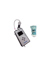
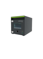
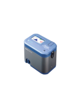
UNISERS 拉曼光譜儀 (DI300 Lab +Raman)
Advantage:
The UNISERS nanocoater enhances the signal-to-noise ratio of particles (defects) on wafers enabling detection limits of 8nm for detection and 50nm for molecular speciation. The coating has a low chemical adhesion to the substrate (wafer) and standard semiconductor wet cleaning chemicals can be used to recycle the wafer.
1. Detection limit: 8nm
2. Molecular speciation down to 50nm
3. True size (material in dependent size estimation)
4. Works on any flat unpatterned wafer including transparent
5. Time and cost efficient workflow: Wafer inspection and review with one tool
6. Small footprint
7. Website: https://unisers.ch/
1. Wafer size : From 1 inch to 12 inch (including wafer coupons)
2. Particle detection limit on unpatterned wafers with RMS roughness <1nm : 8nm
3. Dynamic range : 8nm – 250nm
4. Scanning speed for detection : 8nm mode: 20mins/cm2、25nm mode: 3mins/cm2
5. Particle size estimation reliability : True size estimation (Material-independent)
6. Particle speciation limit : 50nm (Raman)
7. Particle speciation speed : 1s/defect
8. Optical resolution to differentiate two particles (for 20nm particles) : 2 micron
9. Wafer handling : Manual (between two modules)
10. Scanning and signal processing : Automated
1. Defect review with high resolution particle scanning & Raman analysis on area-of-interests.
2. Optimization of CMP-post cleaning processes.
3. Full-wafer inspection of 1- or 2-inch wafers for R&D or witness wafers.
4. All-in-one wafer inspection and defect review for leading-edge fab suppliers and trailing-edge fabs.

